
Fil:Usbkey internals.jpg

Fuld opløsning (1.000 × 959 billedpunkter, filstørrelse: 490 KB, MIME-type: image/jpeg)
|
|
Denne fil er fra Wikimedia Commons. Beskrivelsen af filen fra Commons er gengivet nedenfor. |
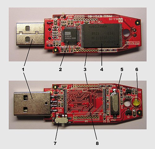
The internal components of a typical keydrive
This photograph shows both sides of the printed circuit board inside a typical keydrive (Seitec USB-BAR USB 1.1circa 2004), in this case an inexpensive 64 Mbyte USB2.0 device. The plastic clamshell case has been removed.
In practice the keydrive consists of only two significant components. The first is the flash memory part (item 4 in the diagram), a generic device that might as easily be found in a digital camera's memory card. The second (item 2 in the diagram) is a device which implements the USB networking and mass-storage interface, and which knows how to make a chunk of generic flash memory appear like a normal disk drive. The high degree of integration in this latter part makes small, inexpensive keydrives possible.
The parts of the device are as follows:
- A male type-A USB connector.
- An Ours Technology Inc. OTi-2168 USB 2.0 mass storage controller. This implements the USB 2.0 host controller, and provides a seamless linear interface to block-oriented serial flash devices, while hiding the complexities of block-orientation, block erasure, and wear balancing. It contains a small RISC microprocessor and a small amount of ROM and RAM. This communicates with the Hynix device over an 8-line unified address/data bus. This version is a 7x7mm 48-pin LQFP (Low Profile Quad Flat Pack) surface-mount device (info).
- JP1 and JP2: two unpopulated 10-pin connectors, used for testing during the keydrive's manufacture.
- A Hynix Semiconductor HY27USxx121M series NAND Flash memory device, featuring 4096 independently erasable blocks each providing 16 Kbytes of storage, yielding a total of 64 Mbytes of usable storage. The version used in this keydrive is a 20x12mm 48-pin TSOP1 (Thin Small Outline Package) surface-mount package (datasheet) archive copy at the Wayback Machine.
- An SKC Shin Chang Electronics 12.000 MHz crystal oscillator (XTAL). The OTi device runs the output of this through a phase-locked loop to produce its main 12 MHz clock signal.
- A single yellow light-emitting diode (run from a pin on the OTi device) which flashes to indicate activity.
- A simple two-position switch, used to indicate whether the device should be in "write-protect" mode. It is shown here in the make position, indicating write-protect is off.
- An unpopulated space for a second TSOP1 memory package. The OTi device is capable of driving up to eight such devices. Having this second space allows the manufacturer to choose (generally on a cost basis) whether to use one or two TSOP flash parts.
Surrounding these main components are a number of tiny surface-mount resistors (many of them serving as pull-ups) and capacitors.
For a closeup of an area of this keydrive, see this image.
Information and licensing
Photographs taken and annotated by John Fader in December 2004 using Adobe Photoshop and Inkscape. This image is (C) Copyright 2004 and (with the exception of its use under the GFDL) all rights are reserved.

|
Tilladelse er givet til at kopiere, distribuere og/eller ændre dette dokument under betingelserne i GNU Free Documentation License', Version 1.2 eller enhver senere version udgivet af Free Software Foundation; uden et invariant afsnit, ingen forsidetekster, og ingen bagsidetekst. En kopi af licensen er inkluderet i afsnittet GNU Free Documentation License. |
| Denne fil er udgivet under Creative Commons Kreditering-Del på samme vilkår 3.0 Ikke-porteret-licensen. | ||
| ||
| Denne licens blev tilføjet som en del af GFDL-licensopdateringen. |
Originally uploaded by John Fader 17:59, 4 December 2004
Filhistorik
Klik på en dato/tid for at se filen som den så ud på det tidspunkt.
| Dato/tid | Miniaturebillede | Dimensioner | Bruger | Kommentar | |
|---|---|---|---|---|---|
| nuværende | 7. jul. 2008, 13:23 | | 1.000 × 959 (490 KB) | Samulili | better |
| 5. apr. 2008, 15:43 |  | 1.000 × 902 (219 KB) | Talgraf777 | {{Information |Description= |Source= |Date= |Author= |Permission= |other_versions= }} | |
| 18. jul. 2005, 21:32 |  | 1.000 × 959 (490 KB) | Solipsist~commonswiki | ==The internal components of a typical keydrive== This photograph shows both sides of the printed circuit board inside a typical keydrive (circa 2004), in this case an inexpensive 64 Mbyte USB2.0 device. The plastic clamshell case has been remov |
Filanvendelse
Den følgende side bruger denne fil:
Global filanvendelse
Følgende andre wikier anvender denne fil:
- Anvendelser på af.wikipedia.org
- Anvendelser på ar.wikipedia.org
- Anvendelser på az.wikipedia.org
- Anvendelser på ba.wikipedia.org
- Anvendelser på bg.wikipedia.org
- Anvendelser på bn.wikipedia.org
- Anvendelser på bs.wikipedia.org
- Anvendelser på ca.wikipedia.org
- Anvendelser på cs.wikipedia.org
- Anvendelser på el.wikipedia.org
- Anvendelser på en.wikipedia.org
- USB flash drive
- File talk:Usbkey internals.jpg
- User talk:John Fader
- Wikipedia:Picture of the day/July 2005
- Wikipedia:Featured picture candidates/May-2005
- Wikipedia:Featured picture candidates/Usbkey internals.jpg
- Wikipedia:Wikipedia Signpost/2005-05-30/Features and admins
- Wikipedia:Today's second feature/July 2005
- Wikipedia:Picture of the day/July 31, 2005
- Wikipedia:POTD/July 31, 2005
- Wikipedia:Today's second feature/July 31, 2005
- User:Cyde/Featured pictures
- User talk:Deltabeignet/Archive01
- Talk:Maxwell's equations/Archive 2
- Portal:Electronics/Selected picture
- Wikipedia:Featured picture candidates/delist/2007
- Portal:Electronics/Selected picture/2
- Wikipedia:Featured picture candidates/delist/USB flash drive
- Wikipedia:Wikipedia Signpost/Single/2005-05-30
- Anvendelser på en.wikibooks.org
- A-level Computing 2009/AQA/Computer Components, The Stored Program Concept and the Internet/Hardware Devices/Secondary storage devices
- A-level Computing 2009/AQA/Print version/Unit 2
- A-level Computing/AQA/Computer Components, The Stored Program Concept and the Internet/Hardware Devices/Secondary storage devices
- A-level Computing/AQA/Print version/Unit 2
- A-level Computing/AQA/Paper 2/External hardware devices/Secondary storage devices
- Anvendelser på es.wikipedia.org
- Anvendelser på es.wikibooks.org
- Anvendelser på et.wikipedia.org
- Anvendelser på eu.wikipedia.org
- Anvendelser på fa.wikipedia.org
- Anvendelser på fi.wikipedia.org
- Anvendelser på fr.wikipedia.org
- Anvendelser på fr.wikibooks.org
- Anvendelser på gl.wikipedia.org
- Anvendelser på he.wikipedia.org
- Anvendelser på hi.wikipedia.org
- Anvendelser på hu.wikipedia.org
- Anvendelser på id.wikipedia.org
Vis flere globale anvendelser af denne fil.